6 / 32
Squeezing a Dense PCB Into a Compact Two-Board Stack
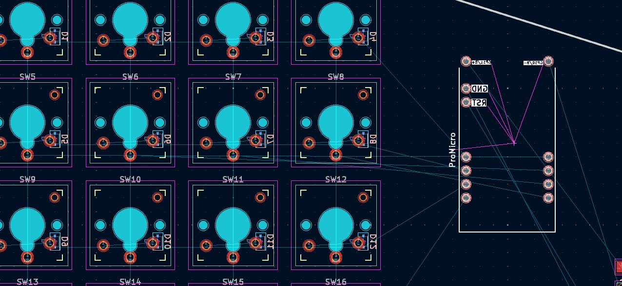
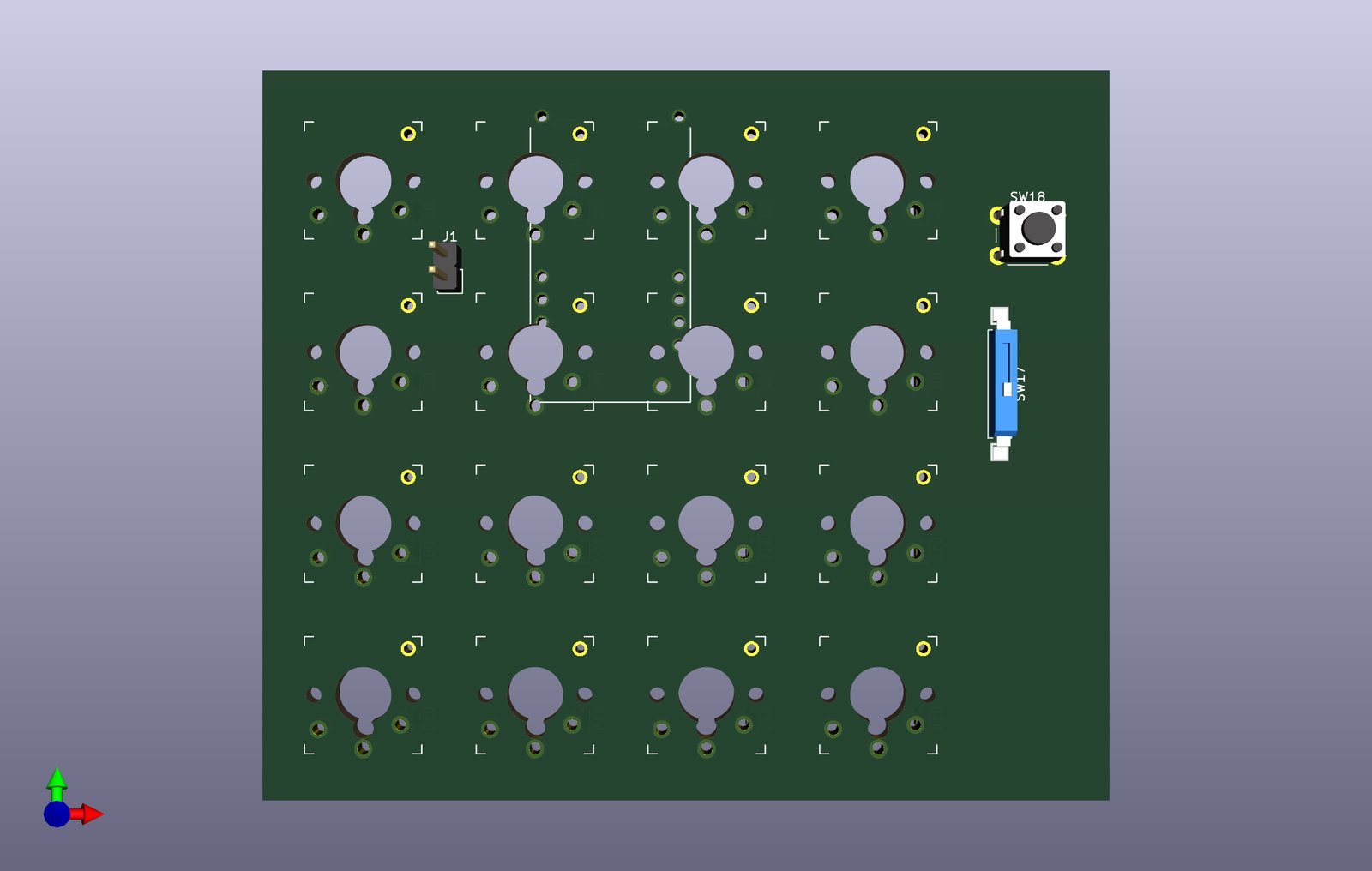
I set out to lay out a PCB from my schematic in as compact a footprint as possible, which turned out to be the hard part of the whole project. The density made routing a real fight — I trimmed the design down by removing pins I didn't need, and split the circuit across two boards connected by headers to take advantage of the vertical space I had available. Even then, the second board was dense enough that I struggled to route its pins, and for a while I wasn't sure it would fit at all. I eventually found a solution, and the plan is to finish routing and order a few boards.
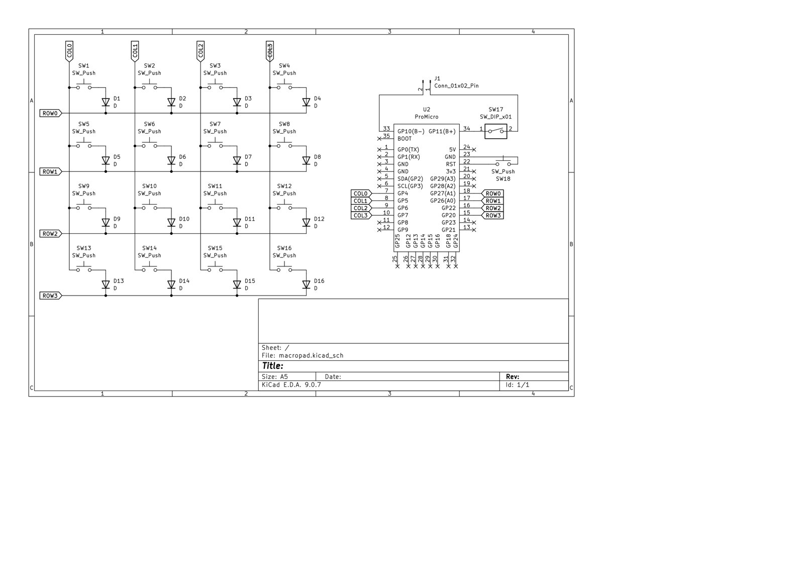
Description
This project started with a PCB schematic I'd put together and a hard constraint: I wanted the finished thing to be compact. Getting from schematic to layout was where the real difficulty showed up. The board is dense, and fitting everything into the footprint I had in mind caused significant issues almost immediately.
The first thing that helped was realising I could simply remove the pins I didn't need. That cleared out some of the clutter, but it didn't solve the underlying problem — I still wasn't sure I could make the whole thing fit.
The approach I settled on was splitting the design across two PCBs connected via headers, making use of the vertical space rather than trying to cram everything into a single flat footprint. That was already the direction I was heading, but it didn't make the routing easy. The boards are dense enough that I hit a wall trying to route the pins on the second PCB, and for a while it looked like it might not come together.
I did eventually find a solution to the routing problem. The next step is to finish routing it tonight and order a few boards so I can see how the stack works in practice.
Gallery
2 images